
Translating step 12
Step 12


-
The raised mesa-looking shapes in the magnified cross-section view (second image) are the transistors' structures, and the little pegs running between them are the actually the contacts between layers.
-
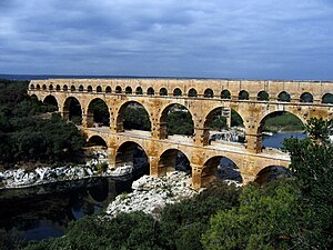
We can't help but think that the transistor layout looks a lot like a Roman aqueduct.
-
This very thin line confirms that this is a 32 nm HKMG (Hi-K metal gate) process.
-
The A6's 32 HKMG process is the same as the one utilized in the [invalid guide link] (APL2498 on Chipworks).
-
In an FET (Field Effect Transistor), K is the dielectric constant of the layer between the gate electrode and the silicon. This is a physical parameter of the material which helps control the turn-on voltage of the transistor